GPU Wars 2016: GTX 1050 Ti & GTX 1050: October 25th
Message boards :
Number crunching :
GPU Wars 2016: GTX 1050 Ti & GTX 1050: October 25th
Message board moderation
| Author | Message |
|---|---|
 shizaru shizaru Send message Joined: 14 Jun 04 Posts: 1130 Credit: 1,967,904 RAC: 0 
|
Finally! My oh my how time flies. It's been 4yrs since GPUs benefitted from a die-shrink. Time for MOAR transistors! Original Thread False Start Teasers & announcements: http://www.anandtech.com/show/9886/amd-reveals-polaris-gpu-architecture http://www.anandtech.com/show/10145/amd-unveils-gpu-architecture-roadmap-after-polaris-comes-vega http://www.techpowerup.com/218898/amd-demonstrates-revolutionary-14-nm-finfet-polaris-gpu-architecture.html http://www.techpowerup.com/218883/4th-generation-graphics-corenext-architecture-codenamed-polaris.html and http://www.techpowerup.com/220372/nvidia-to-unveil-pascal-at-the-2016-computex.html MOAR FLOPs!!! http://www.techpowerup.com/220135/nvidia-gp100-silicon-to-feature-4-tflops-dpfp-performance.html MOAR memory bandwidth: https://devblogs.nvidia.com/parallelforall/nvlink-pascal-stacked-memory-feeding-appetite-big-data/ https://www.techpowerup.com/219527/techpowerup-news-amd-polaris-and-the-memory-war-between-hbm2-and-gddr5x.html MOAR on-screen pixels for GPUs to push because of VR: https://blogs.nvidia.com/blog/2016/03/30/vr-startups/ and new drivers: http://www.anandtech.com/show/10195/oculus-rift-launch-day-news http://www.geforce.com/whats-new/articles/oculus-rift-now-available-and-game-ready https://community.amd.com/community/gaming/blog/2016/03/28/asynchronous-shaders-evolved And a 4yr-old technology that is once again trying to go mainstream: Is Thunderbolt 3 an opportunity for eGPUs (external GPUs) to shine, or do we have to wait a few more years? http://www.anandtech.com/show/10137/razer-core-thunderbolt-3-egfx-chassis-499399-amd-nvidia-shipping-in-april http://www.anandtech.com/show/10188/the-razer-blade-stealth-ultrabook-review http://www.anandtech.com/show/10133/amd-xconnect-external-radeons Pascal in the spotlight April 5th so stay tuned! Hopefully we get an ETA too ;) http://www.gputechconf.com/ ---- Further reading: https://devblogs.nvidia.com/parallelforall/ https://blogs.nvidia.com/blog/2014/03/25/gpu-roadmap-pascal/ https://blogs.nvidia.com/blog/2015/03/17/pascal/ ID: 1775068 · |
|
shizaru Send message Joined: 14 Jun 04 Posts: 1130 Credit: 1,967,904 RAC: 0
|
Official: AMD expects shipments of Polaris architecture-based GPUs to begin in mid-2016 Still on track for a summer release... also: http://www.amd.com/en-us/innovations/software-technologies/25x20 https://youtu.be/5g3eQejGJ_A (Hopefully NVIDIA's Pascal comes soon after. We'll probably have an official ETA this Tuesday.) ID: 1775490 · |
|
shizaru Send message Joined: 14 Jun 04 Posts: 1130 Credit: 1,967,904 RAC: 0
|
If you're willing to sit through a couple of hours of "Deep Learning & Artificial Intelligence", "Self-Driving Cars", and whatever else NVIDIA might be up to in case there's a Pascal announcement then feed goes live in about 5 hours: https://blogs.nvidia.com/blog/2016/04/04/gtc-live/ ID: 1776359 · |
|
shizaru Send message Joined: 14 Jun 04 Posts: 1130 Credit: 1,967,904 RAC: 0
|
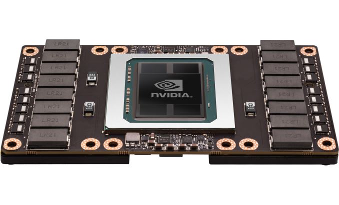 NVIDIA Announces Tesla P100 Accelerator - Pascal GP100 Power for HPC "GP100 is a whale of a GPU, measuring 610mm2 in die size on TSMC's 16nm FinFET process and composed of 15.3B transistors." "With a boost clock of 1.48GHz, altogether Tesla P100 will offer 10.6 TFLOPS of FP32 performance or 5.3 TFLOPS of FP64 performance, more than doubling and tripling Tesla K40's rated throughput on these metrics respectively." "Paired with the GP100 GPU on Tesla P100 is 16GB of HBM2 VRAM, laid out in 4 stacks for a 4096-bit memory bus. NVIDIA quotes P100 as offering 720GB/sec of memory bandwidth, which works out to a memory clock of 1.4Gbps. As we've seen with other HBM products, this marks a significant increase in memory bandwidth, more than doubling NVIDIA's last generation of cards" *** *** Us code/app-challenged folk would love to hear what the volunteer devs have to say about this new memory and what it may (or may not) mean for S@H ;) ID: 1776380 · |
|
shizaru Send message Joined: 14 Jun 04 Posts: 1130 Credit: 1,967,904 RAC: 0
|
With a boost clock of 1.48GHz... That'll probably get "fixed" to "1480MHz" soon (for continuity) ... But the point is: last time we saw frequencies like those was Fermi and the 400/500 series. I wonder if shader clocks are back? Hmmm... I'll see if I can dig up any info.* *Nope, sorry. ID: 1776399 · |
|
shizaru Send message Joined: 14 Jun 04 Posts: 1130 Credit: 1,967,904 RAC: 0
|
Tons more info below, 99.9% over my head ;) Inside Pascal: NVIDIA’s Newest Computing Platform CUDA 8 Features Revealed Maybe our code-whisperers can translate? :P PS Rounding up a bunch of rumors: a 980 successor (aka GP104) might be announced in May/July at around 300mm2 and GDDR5. Oh, and there are a few rumors of a GP102 floating around too (whatever that may be, if true)... ID: 1776423 · |
|
jason_gee Send message Joined: 24 Nov 06 Posts: 7489 Credit: 91,093,184 RAC: 0 
|
*** Us code/app-challenged folk would love to hear what the volunteer devs have to say about this new memory and what it may (or may not) mean for S@H ;) Faster, better, memory subsystem generally makes optimisation easier/simpler, though a lot will depend on the balance of cumpute horsepower to memory bandwidth. Looks like for our purposes, might amount to a near linear double of current generation (for the HBM2 variant), presumably with the GP104 without HBM somewhere in between. "Living by the wisdom of computer science doesn't sound so bad after all. And unlike most advice, it's backed up by proofs." -- Algorithms to live by: The computer science of human decisions. ID: 1776441 · |
Al  Send message Joined: 3 Apr 99 Posts: 1682 Credit: 477,343,364 RAC: 482 
|
From this article: Nvidia drops the Pascal bomb as a Tesla P100 Like Fiji, Nvidia is tapping HBM (High-Bandwidth Memory) for the P100, only they're using HBM2 instead of HBM1. The net result is four layers of stacked memory running on a 4096-bit bus, only the memory this time is running at 1.4Gbps instead of 1.0Gbps, yielding a total memory bandwidth of 720GB/s. That's all well and good, but perhaps more important than simply providing tons of memory bandwidth, HBM2 significantly increases the amount of memory per HBM stack, with P100 sporting a total of 16GB of VRAM. This was obviously a critical factor for Tesla cards, considering the older Tesla K40 already had 12GB of memory, and M40 likewise supports 12GB—not to mention the newly released M40 that comes with 24GB of GDDR5. HBM2 also includes "free" ECC protection, which is a plus for professional applications where reliability and accuracy are paramount. So, maybe we will or maybe we won't get the full monty? Wonder what exactly this all means for those of us crunching here at SETI, especially with the now 3 different types of FP precision available? Major impact, or just an evolutionary step along the way? And love to hear what the pricing will be for the consumer level card, if/when they release one that is pretty much fully enabled?  
ID: 1776478 · |
|
HAL9000 Send message Joined: 11 Sep 99 Posts: 6534 Credit: 196,805,888 RAC: 57
|
*** Us code/app-challenged folk would love to hear what the volunteer devs have to say about this new memory and what it may (or may not) mean for S@H ;) Would you expect that to take advantage of HBM a specialized app would be required? On the Radeon side comparing my R9 390X with GDDR5 to the Fury X with HBM I'm not impressed with the FuryX's run times. With 45% more cores & SP GFLOPS it only manages to run MB tasks 20% faster. SETI@home classic workunits: 93,865 CPU time: 863,447 hours  Join the [url=http://tinyurl.com/8y46zvu]BP6/VP6 User Group[ Join the [url=http://tinyurl.com/8y46zvu]BP6/VP6 User Group[
ID: 1776575 · |
|
rob smith Send message Joined: 7 Mar 03 Posts: 22190 Credit: 416,307,556 RAC: 380 
|
So, maybe we will or maybe we won't get the full monty? Wonder what exactly this all means for those of us crunching here at SETI, especially with the now 3 different types of FP precision available? Major impact, or just an evolutionary step along the way? And love to hear what the pricing will be for the consumer level card, if/when they release one that is pretty much fully enabled? It all depends what you mean by "not getting the full monty" - you will if you (or I) is prepared to pay for it, but it is almost certain that the consumer/domestic devices will be somewhat restricted. The availability of three types of Floating Point precision will make very little difference to SETI as it only uses single precision, although for some other projects this could be a major selling point. One thing to remember is that generally higher precision results in lower processing rates - even when Double Precision is available "on chip". One can but assume that the pricing will be comparable to the current levels of gtx9xx devices, with the usual "launch premium" for early adopters. One thing that will be interesting to keep an eye out for would be the Pascal equivalent to the GTX750, that could be a very cost effective card, given the talk of "xx% more per watt". Bob Smith Member of Seti PIPPS (Pluto is a Planet Protest Society) Somewhere in the (un)known Universe? ID: 1776579 · |
|
Al Send message Joined: 3 Apr 99 Posts: 1682 Credit: 477,343,364 RAC: 482
|
Yeah, it's always been if you want the nicest toys, you'd best have a thich wallet. I guess what I was referring to about the full monty comment is the statement A fully enabled P100 has 60 SMs, giving a potential 3840 cores, but Tesla P100 disables four SMs to give 3584 total cores. Maybe sometime down the road they'll release a fully enabled version, maybe when they get their yields up? Regardless, if they do, you know it won't be cheap.. :-)
ID: 1776663 · |
|
HAL9000 Send message Joined: 11 Sep 99 Posts: 6534 Credit: 196,805,888 RAC: 57
|
Yeah, it's always been if you want the nicest toys, you'd best have a thich wallet. I guess what I was referring to about the full monty comment is the statement Perhaps on the enterprise end they reduce the number used in the event parts of it burn out. Similar to how SSD drives have more flash than is usable. So they can allocate new blocks when flash cells go dead. SETI@home classic workunits: 93,865 CPU time: 863,447 hours Join the [url=http://tinyurl.com/8y46zvu]BP6/VP6 User Group[
ID: 1776673 · |
|
jason_gee Send message Joined: 24 Nov 06 Posts: 7489 Credit: 91,093,184 RAC: 0
|
*** Us code/app-challenged folk would love to hear what the volunteer devs have to say about this new memory and what it may (or may not) mean for S@H ;) In a general sense no app specialised for the memory type should be necessary (or worth it in practical senses). What is slowly happening though, is more codepaths being added, along with self tuning and dispatch, such that optional automatic scaling can take place. I don't know much about the current OpenCL apps or AMDs various implementations, though for the NV-Cuda situation there are substantial portions that are (video) memory bound and PCIe bound. In the first case HBM should help, while the second self scaling and Petri's streaming, giving latency hiding, will help. With Generic code on current hardware yielding ~5% compute efficiency ( Flop/TheoreticalPeakFlops ), a bit more total running multiple instances, the other ~95% is various latencies and bandwidth restriction. I'm fairly confident over time we'll approach 20% (With petri's experimental code reaching ~10% now), at least on the next, current, and maybe back to Fermi class with some diminishing returns. "Living by the wisdom of computer science doesn't sound so bad after all. And unlike most advice, it's backed up by proofs." -- Algorithms to live by: The computer science of human decisions. ID: 1776773 · |
|
Al Send message Joined: 3 Apr 99 Posts: 1682 Credit: 477,343,364 RAC: 482
|
Hey Jason, and anyone else who knows much about this, I just started a thread about OpenCL vs. CUDA, if people who are in the know could add comments to it, that would be helpful in understanding the current situation.
ID: 1776856 · |
|
Bill G Send message Joined: 1 Jun 01 Posts: 1282 Credit: 187,688,550 RAC: 182
|
http://www.pcworld.com/article/3053600/hardware/apples-aging-mac-pro-is-falling-way-behind-windows-rivals.html?token=%23tk.PCW_nlt_pcw_bestof_html_2016-04-08&idg_eid=a0e1f7b61040fb71f0dec4f3f7f091c8&utm_source=Sailthru&utm_medium=email&utm_campaign=Best%20of%20PCWorld%202016-04-08&utm_term=pcw_bestof_html#tk.PCW_nlt_pcw_bestof_html_2016-04-08 Just to add a bit to what is coming (and perhaps going).  SETI@home classic workunits 4,019 SETI@home classic CPU time 34,348 hours ID: 1777173 · |
|
shizaru Send message Joined: 14 Jun 04 Posts: 1130 Credit: 1,967,904 RAC: 0
|
OK so more rumors flying around that a mainstream GP104 chip will get announced (actual availability unknown) at Computex 2016 (from 31st to June 4th). A couple of pictures of the chip are floating around which superficially look authentic: http://www.fudzilla.com/news/graphics/40515-nvidia-gtx-1070-gp104-200-pascal-asic-pictured http://videocardz.com/59266/nvidia-pascal-gp104-gpu-pictured-up-close Even if bogus it would still make sense for the GP104 to be in the ~300mm2 range so here's a... brief history in time :) - GeForce 9800 GTX - 324mm2 - 140W - GeForce GTS 250 - 260mm2 - 150W - GeForce GTX 460 - 332mm2 - 150W or 160W (2 versions) - GeForce GTX 560 Ti - 332mm2 - 170W - GeForce GTX 680 - 294mm2 - 195W - GeForce GTX 770 - 294mm2 - 230W - GeForce GTX 960 - 227mm2 - 120W - GeForce GTX 980 - 398mm2 - 165W So while we wait, I was thinking maybe we could see how these cards behave @Seti. I'll probably have better luck searching for a unicorn but anybody have numbers for v8 (or v7 if not) on stock app doing one WU at a time? Any other ideas for an apples-to-apples comparison? For reference my little ION GPU does a "normal" ~0.43 Angle Range v8 WU in about 3 to 3 and 1/2 hours. Poor thing has a 12W TDP :) As always, above tech specs from: https://en.wikipedia.org/wiki/List_of_Nvidia_graphics_processing_units ID: 1782605 · |
|
Grant (SSSF) Send message Joined: 19 Aug 99 Posts: 13731 Credit: 208,696,464 RAC: 304
|
Any other ideas for an apples-to-apples comparison? The problem is the lack of an application that makes use of the new hardware's abilities. My GTX 750Tis are about on par with the old GTX 460 and a bit behind the GTX560Ti because of the changes in architecture that result in the current applications being nowhere nearly as effective on the new hardware as they were on the old. As far as power consumptions is concerned they leave the old hardware for dead. And I suspect that with an application that takes advantage of the new hardware, and is able to work around it's quirks (and particularly the current drivers) it's performance would leave the old hardware far behind as well. Grant Darwin NT ID: 1782606 · |
|
jason_gee Send message Joined: 24 Nov 06 Posts: 7489 Credit: 91,093,184 RAC: 0
|
Any other ideas for an apples-to-apples comparison? It's going to be an interesting few months leading up to Pascal. Seeing as we have a lot of new code going in, it's starting to look like some precautions/safeties, at least for default/stock operation are going to be warranted to make sure stuff doesn't break in the middle of all the tech changes going on (Drivers, GPUs, OSes, and seti processing all changing ) Having to supply these things with Fire extinguishers and miniature fusion power plants probably isn't going to work, lol. "Living by the wisdom of computer science doesn't sound so bad after all. And unlike most advice, it's backed up by proofs." -- Algorithms to live by: The computer science of human decisions. ID: 1782610 · |
|
shizaru Send message Joined: 14 Jun 04 Posts: 1130 Credit: 1,967,904 RAC: 0
|
changes in architecture that result in the current applications being nowhere nearly as effective on the new hardware as they were on the old. I could be overoptimistic or oversimplifying or both but: For now I can't think of (or better, don't know of) a reason that couldn't change overnight. If Pascal's architecture is closer to Fermi and the 460 or 560Ti then I'm guessing the Pascal drivers could roll back into Seti app favor. That's not to say that the old apps necessarily work "out the gate", rather that they happen to be better optimized for Pascal rather than Kepler. If that makes sense :) (I kinda got the impression, in hindsight, that Fermi architecture was 100% compute oriented and then intentionally watered down over generations for the sake of gaming & efficiency. Pascal looks to be the same if GeForce cards end up anything like the Tesla that was announced. In other words this could be Fermi 2.0 and it again gets watered down over the generations. It looks like compute gets the advantage this round. Reminder: you guys notice that jump in frequencies on Pascal?) ID: 1782626 · |
|
shizaru Send message Joined: 14 Jun 04 Posts: 1130 Credit: 1,967,904 RAC: 0
|
I'll probably have better luck searching for a unicorn but anybody have numbers for v8 (or v7 if not) on stock app doing one WU at a time? That was poorly written. What I meant was anybody have v8 times for any of these: - GeForce 9800 GTX - 324mm2 - 140W - GeForce GTS 250 - 260mm2 - 150W - GeForce GTX 460 - 332mm2 - 150W or 160W (2 versions) - GeForce GTX 560 Ti - 332mm2 - 170W - GeForce GTX 680 - 294mm2 - 195W - GeForce GTX 770 - 294mm2 - 230W - GeForce GTX 960 - 227mm2 - 120W - GeForce GTX 980 - 398mm2 - 165W ID: 1782630 · |

©2024 University of California
SETI@home and Astropulse are funded by grants from the National Science Foundation, NASA, and donations from SETI@home volunteers. AstroPulse is funded in part by the NSF through grant AST-0307956.